 Q. No.
A transistor is operated in common emitter configuration at When base current is changed from 10mA to 30mA, it produces a change in emitter current from 2A to 4A, the current amplification factor is
1. 100
2. 99
3. 10
4. 9
एक ट्रांजिस्टर उभयनिष्ठ उत्सर्जक विन्यास में पर संचालित किया जाता है। जब आधार धारा को 10mA से 30mA में परिवर्तित किया जाता है, तब यह उत्सर्जक धारा में 2A से 4A का परिवर्तन उत्पन्न करता है। धारा प्रवर्धन कारक है
1. 100
2. 99
3. 10
4. 9


The current through an ideal p-n junction diode shown in the circuit will be -
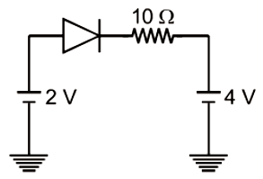
1. 5 A
2. 0.2 A
3. 0.6 A
4. Zero
परिपथ में दर्शाए गए आदर्श p-n संधि डायोड में धारा की गणना कीजिए।
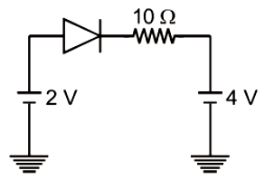
1. 5 A
2. 0.2 A
3. 0.6 A
4. शून्य
In the given circuit power developed in \(1 k \Omega\) resistor is
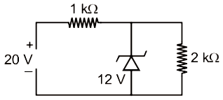
1. 36 mW
2. 12 mW
3. 144 mW
4. 64 mW
दिए गए परिपथ में \(1 k \Omega\) प्रतिरोधक में उत्पन्न शक्ति है:
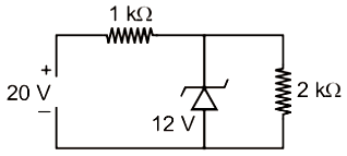
1. 36 mW
2. 12 mW
3. 144 mW
4. 64 mW


In a common emitter transistor amplifier, the audio signal vlotage across the collector is 3V. The resistance of collector is 3k. If current gain is 100 and the base resistance is 2k, the voltage and power gain of the amplifier is
| 1. | 200 and 1000 | 2. | 15 and 200 |
| 3. | 150 and 15000 | 4. | 20 and 2000 |
उभयनिष्ठ उत्सर्जक ट्रांजिस्टर प्रवर्धक में, संग्राहक पर वोल्टेज 3V है। संग्राहक का प्रतिरोध 3k है। यदि धारा लाभ 100 है और आधार प्रतिरोध 2k है, प्रवर्धक का वोल्टेज और शक्ति लाभ ज्ञात कीजिए।
| 1. | 200 और 1000 | 2. | 15 और 200 |
| 3. | 150 और 15000 | 4. | 20 और 2000 |
The given circuit has two ideal diodes connected as shown in the figure below. The current flowing through the resistance will be

| 1. | 2.5 A | 2. | 10.0 A |
| 3. | 1.43 A | 4. | 3. 13 A |
दिए गए परिपथ में दो आदर्श डायोड को आरेख में दर्शाए गए अनुसार जोड़ा गया है। प्रतिरोध में प्रवाहित होने वाली धारा कितनी होगी?
| 1. | 2.5 A | 2. | 10.0 A |
| 3. | 1.43 A | 4. | 3. 13 A |


The given graph represents V-I characteristic for a semiconductor device. Which of the following statement is correct?

| 1. | It is V-I characteristic for solar cell where point A represents open circuit voltage and point B short circuit current |
| 2. | It is for a solar cell and points A and B represent open circuit voltage and current, respectively |
| 3. | It is for a photodiode and points A and B represent open circuit voltage and current, respectively |
| 4. | It is for a LED and points A and B represents open circuit voltage and short circuit current respectively |
दिया गया ग्राफ अर्धचालक उपकरण के लिए V-I अभिलक्षणिक को दर्शाता है। निम्नलिखित में से कौन सा कथन सही है?
| 1. | यह सौर सेल के लिए V-I अभिलक्षणिक है, जहां बिंदु A विवृत परिपथ वोल्टता और बिंदु B लघु परिपथ धारा को दर्शाता है। |
| 2. | यह सौर सेल के लिए V-I अभिलक्षणिक है और बिंदु A और B क्रमशः विवृत परिपथ वोल्टता और विवृत परिपथ धारा को दर्शाते हैं। |
| 3. | यह फोटोडायोड के लिए V-I अभिलक्षणिक है और A और B क्रमशः विवृत परिपथ वोल्टता और विवृत परिपथ धारा को दर्शाते हैं। |
| 4. | यह LED के लिए V-I अभिलक्षणिक है और A और B क्रमशः विवृत परिपथ वोल्टता और लघु परिपथ धारा को दर्शाते है। |
The output (x) of logic circuit shown in figure will be

1.
2.
3.
4.
आरेख में दर्शाए गए लॉजिक परिपथ का निर्गत (x) होगा -
1.
2.
3.
4.
C and Si both have same lattice structure,having 4 bonding electrons in each.However, C is insulator whereas Si is intrinsic semiconductor. This is because
| 1. | in case of C, the valence band is not completely filled at absolute zero temperature |
| 2. | in case of C,the condition band is partly filled even at absolute zero temperature |
| 3. | the four bonding electrons in the case of C lie in the second orbit,Whereas in the case of Si they lie in the third |
| 4. | the four bonding electrons in the case of C lie in the third orbit, whereas for Si they lie in the fourth orbit |
C और Si दोनों में समान जालक संरचना है, जिसमें प्रत्येक में 4 बंधित इलेक्ट्रॉन हैं। हालांकि, C विद्युतरोधी है जबकि Si नैज अर्धचालक है। यह किस कारण है?
| 1. | C की स्थिति में संयोजकता बैंड परम शून्य ताप पर पूर्ण रूप से भरा नहीं होता है। |
| 2. | C की स्थिति में चालक बैंड परम शून्य ताप पर भी आंशिक रूप से भरा हुआ होता है। |
| 3. | C की स्थिति में चार बंधित इलेक्ट्रॉन दूसरी कक्षा में स्थित हैं, जबकि Si की स्थिति में वे तीसरी कक्षा में स्थित हैं। |
| 4. | C की स्थिति में चार बंधित इलेक्ट्रॉन तीसरी कक्षा में स्थित हैं, जबकि Si की स्थिति में वे चौथी कक्षा में स्थित हैं। |


Transfer characteristic [output voltage vs input voltage ] for a base biased transistor in CE configuration is as shown in the figure.For using transistor as a switch, it is used

1. in region III
2. both in region (I) and (III)
3. in region II
4. in region I
उभयनिष्ठ उत्सर्जक विन्यास में आधार बायस ट्रांजिस्टर के लिए स्थानांतरण अभिलक्षण [निर्गत वोल्टता बनाम निवेशी वोल्टता ] आरेख में दर्शाए गए अनुसार है। ट्रांजिस्टर का उपयोग स्विच के रूप में करने के लिए, यह उपयोग किया जाता है -
1. क्षेत्र III में
2. (I) और (III) दोनों क्षेत्र में
3. क्षेत्र II में
4. क्षेत्र I में

© 2026 GoodEd Technologies Pvt. Ltd.