
 Q. No.
In a semiconducting material, the mobilities of electrons and holes are \(\mu_e\) and \(\mu_{h}\) respectively. Which of the following is true?
1. \(\mu_{e} > \mu _{h}\)
2. \(\mu_{e} < \mu _{h}\)
3. \(\mu_{e} = \mu _{h}\)
4. \(\mu_{e} <0; ~\mu _{h}>0\)
1. \(\mu_{e} > \mu _{h}\)
2. \(\mu_{e} < \mu _{h}\)
3. \(\mu_{e} = \mu _{h}\)
4. \(\mu_{e} <0; ~\mu _{h}>0\)


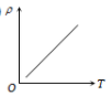
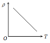
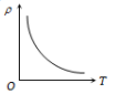
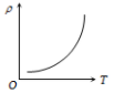
The temperature (T) dependence of resistivity () of a semiconductor is represented by
1. 
2. 
3. 
4. 
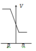
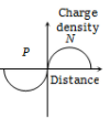
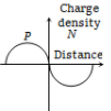
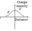
In a forward biased P-N junction diode, the potential barrier in the depletion region is of the form
1. 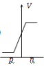
2. 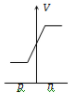
3. 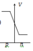
4. 


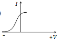
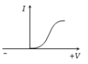
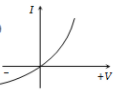
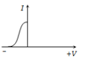
Different voltages are applied across a P-N junction and the currents are measured for each value. Which of the following graphs is obtained between voltage and current?
1. 
2. 
3. 
4. 
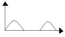
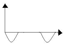
If the following input signal is sent through a PN-junction diode, then the output signal across will be
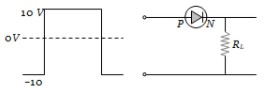
1. 
2. 
3. 
4. 


The resistance of a germanium junction diode whose is shown in figure is
(1) 5 k
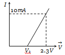
(2) 0.2 k
(3) 2.3 k
(4)
In the half-wave rectifier circuit shown. Which one of the following wave forms is true for , the output across C and D?
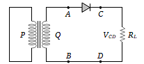
| 1. | 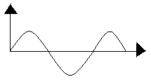 |
2. |  |
| 3. | 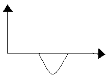 |
4. |  |
A full-wave rectifier circuit along with the input and output voltages is shown in the figure.

The contribution to the output voltage from diode – 2 is :
(1) A, C
(2) B, D
(3) B, C
(4) A, D


The i-V characteristic of a P-N junction diode is shown below. The approximate dynamic resistance of the P-N junction when a forward bias of 2 volt is applied

(1) 1
(2) 0.25
(3) 0.5
(4) 5
© 2025 GoodEd Technologies Pvt. Ltd.